How is Component Placement Optimized in PCB Assembly?
Component Placement Optimized in PCB Assembly
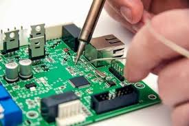
The first step in creating a circuit board is to create the schematic design, which is the diagram that shows how each component connects to other components and to the grounding wire. This is then translated into a physical layout that is ready for the manufacturing process. Once the design is complete, specialized machines will begin placing each component into its designated location on the pcb circuit board assembly. These machines are highly programmable and can achieve high speeds, which makes them ideal for large production runs. They are also designed to eliminate human error, which can be very costly for any company.
Whether the production method is manual or automated, the PCB layout must be optimized for assembly and diagnostics. This can be done by ensuring that all components are located in the correct place and that they have enough space to move freely. In addition, it is important to keep the layout as clean as possible. This will reduce signal integrity issues and minimize EMI, which can cause malfunctions.
How is Component Placement Optimized in PCB Assembly?
To ensure a smooth assembly process, the components must be grouped together and positioned in a way that facilitates heat dissipation. This is especially important for components that generate a lot of heat, such as processors. In most cases, they should be placed in the center of the board, which promotes even heat distribution, avoiding localized hot spots. It is also important to keep these types of components far away from any sensitive parts that may become damaged by the heat.
Other considerations include orienting the components in structured rows and columns, which simplifies assembly by pick-and-place machines and increases efficiency during inspection and maintenance. Indicating the polarity of a component on its silkscreen is also a must for easy identification during manufacturing and troubleshooting. It is recommended that there be at least 40mil of space between each component and 100mil of clearance from the edge of the board.
Finally, the placement of the power and ground planes is also important. In most cases, the ground and power should be separated as much as possible, as this will minimize EMI. It is also necessary to avoid crossing signals over each other, which can lead to interference and noise. Lastly, it is crucial to design a power supply with enough current capacity to meet the device’s requirements. To do so, it is a good idea to provide multiple vias at every layer transition. This will not only maximize current capacity, but it will also reduce resistive losses and inductance. This is one of the best ways to increase the reliability of a circuit board.